


It is very fortunate sometimes to meet people who have a passion to create new things and to improve on the methods to make them. This post is about Paul Steinmeyer’s adventure in creating PCB’s using his new J Tech 2.8W laser upgrade kit. Paul is a Health Physicist specializing in electronics and software design at Radiation Safety Associates, Inc. During this process we partnered up and developed the new SW product, LaserEtch. This new tool can take a bitmap image and very quickly raster the laser over a work surface to either mark and engrave, or to remove material. It was developed for this PCB process, but it has many more applications.
Here is his story and tutorial for making PCB’s:
[quote]I have an old Solidoodle 3 3D printer that was no longer extruding properly. I got a new, higher end printer and wanted to do something with the old Solidoodle. I got the idea to mount a laser in order to create circuit boards from several places on the internet, and thought that would be an excellent use. After spending several enjoyable evenings reading through laser forums and Ebay listings I stumbled across the J Tech Photonics web site and discovered their high-powered laser upgrades for 3D printers. The price was fair and the equipment was excellent. There were no problems at all in mounting, powering, and controlling the laser in place of the extruder.
While a 2.8 watt laser is quite powerful, it cannot directly etch copper. What it can do is burn off a black spray-paint coating from a piece of copper clad, and then be etched by normal means.
The Inkscape plug-in provided by J Tech Photonics worked very well for making text and relatively simple printed circuit boards, but really only traces outlines. I prefer much more control over spacing between traces, and where and how much copper to leave behind. Especially when dealing with higher voltages, simple outlines and thin lines are not always sufficient.
LaserEtch was written to fill that need. It takes bitmap files and converts them into the g-code used by most 3D printers. The speed is optimized by moving the laser quickly when it isn’t turned on and slowly when it is. These speeds are in the control of the user. Also, although true rastering is available, the default mode optimizes the travel of the laser head. There is no point in moving the laser all the way to one edge and back if there is nothing to be “burned” while on that path.
A Note About Safety
Lasers can hurt you if used improperly, potentially badly and potentially permanently. Always use appropriate eye protection, do not allow the beam to come into contact with anything that you don’t want heated or burned (like your hand), etc.
Be aware that burned paint fumes (that is, the small particulates generated when paint is heated enough that it smokes) can be particularly nasty. They are of such size that they can become embedded in your lungs and your body has no mechanism for removing them (roughly similar to asbestos). Whatever you choose to cut or burn with your laser, be sure to use adequate ventilation or other appropriate respiratory protection!
Coat Your Copper Clad
Since the paint takes a little while to dry I suggest starting by preparing and painting the copper clad. Clean the copper clad with water and a mild detergent, then wipe dry. I have not found it necessary to sand or otherwise buff the board.
Use a fast drying Flat Black Matte finish paint. Examples of two paints that work well are shown in the below picture. Flat black does seem to work better than glossy, as it absorbs the energy from the laser more completely. Apply the paint evenly and gently. Enough to completely cover the copper but not too thick. Allow to dry completely.


Since spray painting takes a little time effort to put together (and clean up from afterwards) I tend to paint all the copper clad I have in one shot. It seems to keep very well as long as no paint is scraped off the material while in storage.
Create the Layout
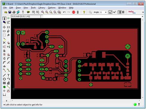
I’m using Eagle version 6.6.0 for schematic capture and layout. The process described here should be similar to that used for any other program.
It is worth noting that the part of the process that burns paint off of copper clad seems to be far more precise than chemical etching is. Very small traces (e.g., ~0.01”) that are easily created on the board by the laser do not always survive the etching process. I try to use a minimum trace width of 0.016” whenever possible. Similarly, the annular rings around through-hole features should be somewhat larger than required by a commercial board house.
Convert Layout to Image
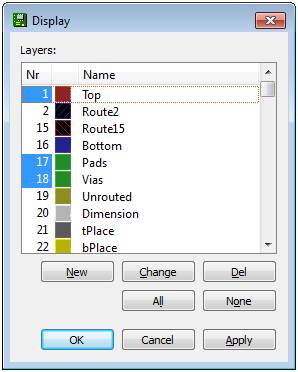
You should first turn off the display of any layers that are not part of what should be in the print file. For my Eagle conventions I leave on only the Top, Pads, and Vias layer.
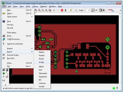
The next step is to export the file as an image, using File|Export|Image in Eagle, and you will be asked to give the file a name and have the opportunity to set the resolution.
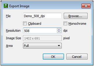
The resolution (expressed as dots per inch or dpi) you use depends a lot on how fine you want the detail to be versus how long you are willing to wait while the laser burns the board.
I tend to use American units (i.e., inches) when I create layouts but my Solidoodle is set up for metric (i.e., mm), I try to use a resolution that will convert easily. Since there are 25.4 mm in an inch, I use multiples of 254. For my own purposes I’ve found twice that, or 508 dpi, to work well.
Converting the Image to a Bitmap
Eagle saves the image file in the *.png format. Fortunately, the Paint application (included in Windows) can easily convert *.png files into bitmaps (*.bmp). There are any number of other graphics editors that can also do the job. “Paint.net” is a very good (and free) application that comes highly recommended by some. Anyway, open the image file created by Eagle in Paint or another graphics editor of your choice.
While open in Paint (or whatever), take the opportunity take a good look at the image. When being burned, the laser will be powered on over all portions where the color is black, and the laser will be off for all other colors.
Looking at the image below you can see that Eagle has put the ends of traces (red) inside of the vias (green). This would result in copper covering areas where you’d like to drill. There is also a black border around the edge. Forcing the laser to burn this ends up adding substantially to the amount of time needed to burn the board.
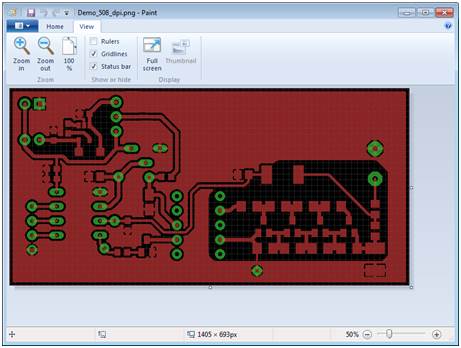
I go through the image at a fairly high magnification and, using the fill tool, convert the outside border to red. I fill all the via holes with black, and then take a careful look for anywhere that the traces look too thin, spacing too close, etc. and make adjustments and repairs.

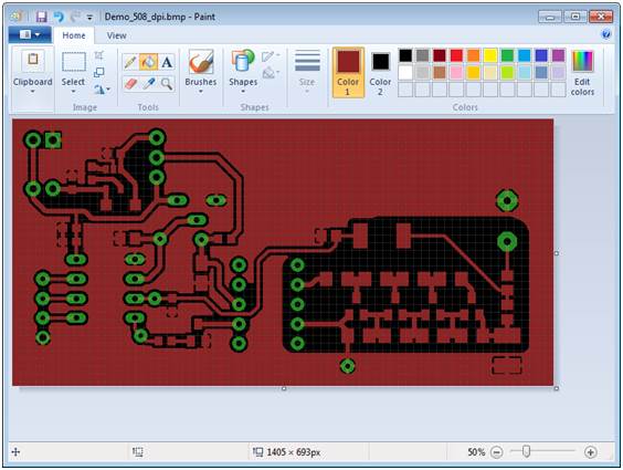
Finally, use the Save As BMP Picture function.
Convert to G-Code
Start up LaserPCB and use the “Load BMP” button to, well, load the bitmap you just saved. It will appear in the main window, sized to be as large as possible. You can maximize this window to make it as large as possible.
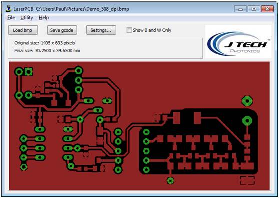
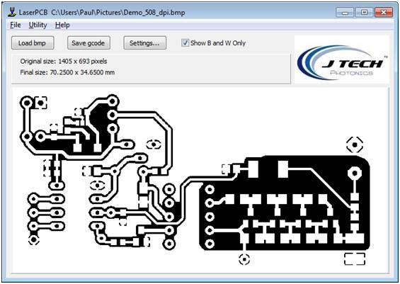
Also, checking the “Show B and W Only” will provide a representation of exactly how the image will be printed.
Click the “Settings…” button to bring up the settings window.
LaserEtch installs with a few default “profiles.” Above I’ve pressed “Load Profile” and loaded the profile for PCBs. Note that these are settings profiles that have worked well for me but may not be optimum for you. Adjust them as needed as you gain experience. The laser commands shown are correct for the Solidoodle where the laser power is controlled by the adjustment for fan speed.
The laser etching process is actually quite forgiving. If the laser does not burn the paint off sufficiently you can just repeat the process, provided of course that you haven’t moved the piece. And because the laser can’t actually etch the copper there is little risk of overdoing it. If all fails anyway, the paint can be wiped off the board to be repainted and used again for another try.
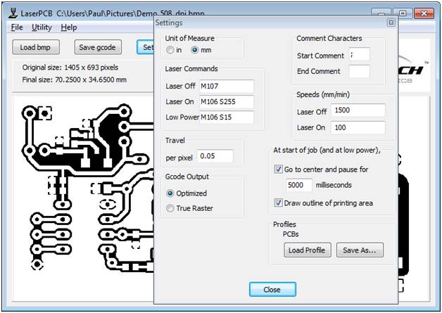
The Travel parameter is essentially the size of a pixel in the final output. Keep in mind that you can only really change the width of a pixel. The height will be dictated by the size of the laser’s focused beam.
Through experimentation I’ve found that 0.05 mm per pixel works well for my laser. That’s the reason I specified 508 dpi, so that using a travel of 0.05 mm makes the final image size the same as it was designed to be in Eagle.
The Gcode output should pretty much always be “Optimized.” Using a semicolon is fairly standard for comments (with nothing required for the ending).
I’ve found 1500 mm/min to be a good speed for when the laser is off. It is fast enough that it doesn’t waste time but slow enough that it can still slow down instantly, with no discernable backlash, when the laser turns on.
The laser on speed of 100 mm/min is fairly conservative, but I’d rather have the print be a little slow than have to repeat it.
When you are happy with your settings, close the Settings window and press the “Save gcode” button. After a few moments (depending on the size and complexity of the bitmap file) you will be prompted to save the gcode file.
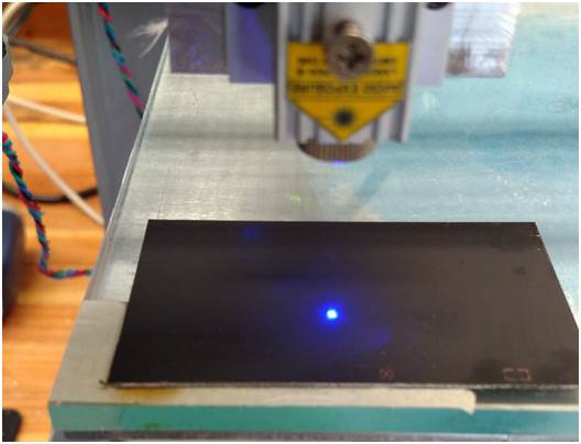
There are a couple of options for what occurs at the start of the print. The first one, “Go to the center and pause for” will do just that. The printer will go to the 0,0 position, move to the exact center of the area to be printed, and then pause there for the amount of time indicated with the laser on at the Low Power setting. This gives you the opportunity to make sure your material is in the right place, and if not, you have the opportunity to pause the print job and re-center. The second option, “Draw outline of printing area,” sets the laser to the low power setting and traces where the perimeter will be. Again, this just gives you the opportunity to make sure your material is properly positioned.
Time to Print
Finally! Here is the laser pausing (at low power) over the center of the print area.
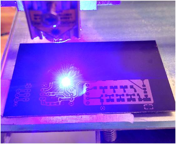
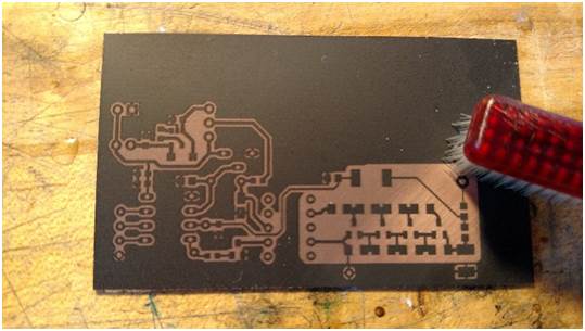
This shows the piece about 75% complete. The laser is at full power and doing a pretty good job of removing the paint from the copper.
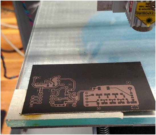
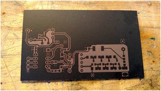
Here the print is finished, still sitting on the Solidoodle print bed…
…and on the bench.
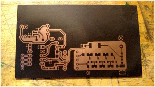
The laser-burning process still leaves some residue on the copper that can interfere with the etching process. I’ve tried many things and scrubbing it gently with a toothbrush seems to work the best. It removes the residue without taking off any of the unburned paint.
Here it is after finishing cleaning it with the toothbrush.
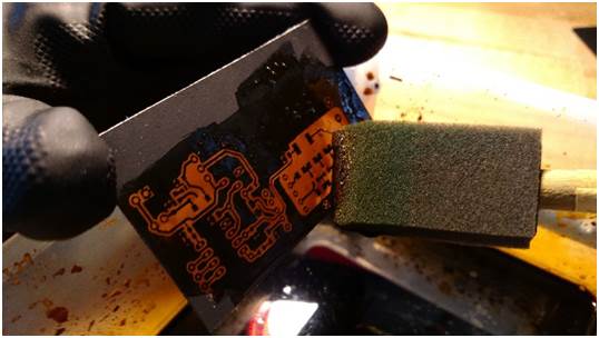
Etch away the exposed copper using your preferred method. I use (and re-use and re-use) ferric chloride as the etchant. With cheap sponge brush, I gently wipe the etchant on the copper.
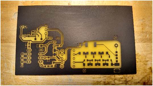
Etching complete.
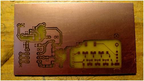
Remove remaining paint with acetone.
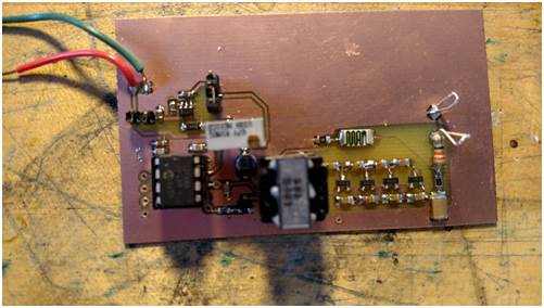
Populate the board.
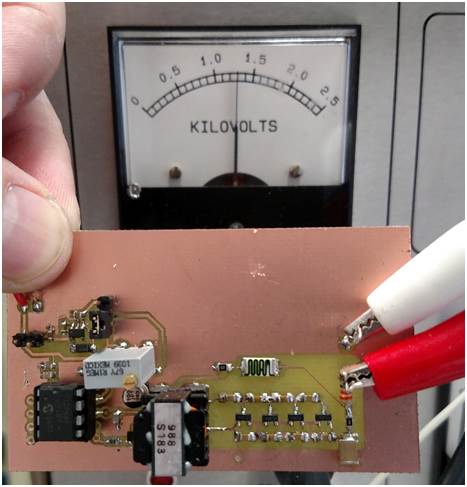
And it works!
Just curious if this process can be done with the 2 W (1.7) laser I recently purchased? If so, what speeds would you recommend with it?
It depends a bit on your paint you are using and the thickness of your application, but it should work. Try going at 50mm/min and see how it goes. If it doesn’t take it all off, then slow it down some more. If it works great, then speed it up until you get it just not working then scale it back in speed 10% to find the sweet spot with your paint choice.
Were i download laserpcb software? link please?
The laser etch download is on the bottom of the product page: Laser Etch Software
Is there a list of proper setting values for the 3.8w laser configuration?
Hi there. Is there a way that you can share the schematic of your board? Thanks in advance.
Rather than burn off a paint layer you can use dry film positive photo resist. It’s inexpensive and you can run it at a much lower power.
Could this be done with a 1w laser kit?